|
Encapsulation Solder of Diode Laser Bar Stacks |
AuSn Packed |
|
Central Wavelength |
1064nm |
|
Output Power |
≥55W |
|
Working Current |
≤30 A |
|
Working Voltage |
≤24V |
|
Working Mode |
CW |
|
Cavity Length |
900mm |
|
Output Mirror |
T = 20% |
|
Water Temperature |
25±3℃ |
Subscribe to Our Social Media For Prompt Post
Abstract
The demand for CW (Continuous Wave) diode-pumped laser modules is increasing rapidly as an essential pumping source for solid-state lasers. These modules offer unique advantages to meet the specific requirements of solid-state laser applications. G2 - A Diode Pump Solid State Laser, the new product of the CW Diode Pump Series from LumiSpot Tech, has a wider application field and better performance abilities.
In this article, We will include content focusing on the product applications, product features, and product advantages regarding the CW diode pump solid-state laser. At the end of the article, I will demonstrate the test report of the CW DPL from Lumispot Tech and our special advantages.
The Application Field
High-power semiconductor lasers are mainly used as pump sources for solid-state lasers. In practical applications, a semiconductor laser diode-pumping source is key to optimizing the laser diode-pumped solid-state laser technology.
This type of laser utilizes a semiconductor laser with a fixed wavelength output instead of the traditional Krypton or Xenon Lamp to pump the crystals. As a result, this upgraded laser is called the 2nd generation of CW pump laser (G2-A), which has the characteristics of high efficiency, long service life, good beam quality, good stability, compactness and miniaturization.

High-Power Pumping Ability
CW Diode Pump Source offers an intense burst of optical energy rate, effectively pumping the gain medium in the solid-state laser, to realize the best performance of the solid-state laser. Also, its relatively high peak power(or average power) enables a wider range of applications in industry, medicine, and science.
Excellent Beam and stability
CW semiconductor pumping laser module has the outstanding quality of a light beam, with stability spontaneously, which is crucial to realize the controllable precise laser light output. The modules are designed to produce a well-defined and stable beam profile, ensuring reliable and consistent pumping of the solid-state laser. This feature perfectly meets the demands of laser application in industrial material processing, laser cutting, and R&D.
Continuous Wave Operation
The CW working mode combines both merits of continuous wavelength laser and Pulsed Laser. The main difference between CW Laser and a Pulsed laser is the power output. CW laser, which is also known as a Continuous wave laser, has the characteristics of a stable working mode and the ability to send a continuous wave.
Compact and Reliable Design
CW DPL can be easily integrated into the current solid-state laser depending on the compact design and structure. Their robust construction and high-quality components ensure long-term reliability, minimizing downtime and maintenance costs, which is especially important in industrial manufacturing and medical procedures.
The Market Demand of the Series of DPL - Growing Market Opportunities
As the demand for solid-state lasers continues to expand across different industries, so does the need for high-performance pumping sources such as CW diode-pumped laser modules. Industries like manufacturing, healthcare, defense, and scientific research rely on solid-state lasers for precision applications.
To sum up, as the diode pumping source of the solid-state laser, the characteristics of the products: high-power pumping capability, CW operation mode, excellent beam quality and stability, and compact-structured design, increase the market demand in these laser modules. As the supplier, Lumispot Tech also puts plenty of effort into optimizing the performance and technologies applied in the DPL series.
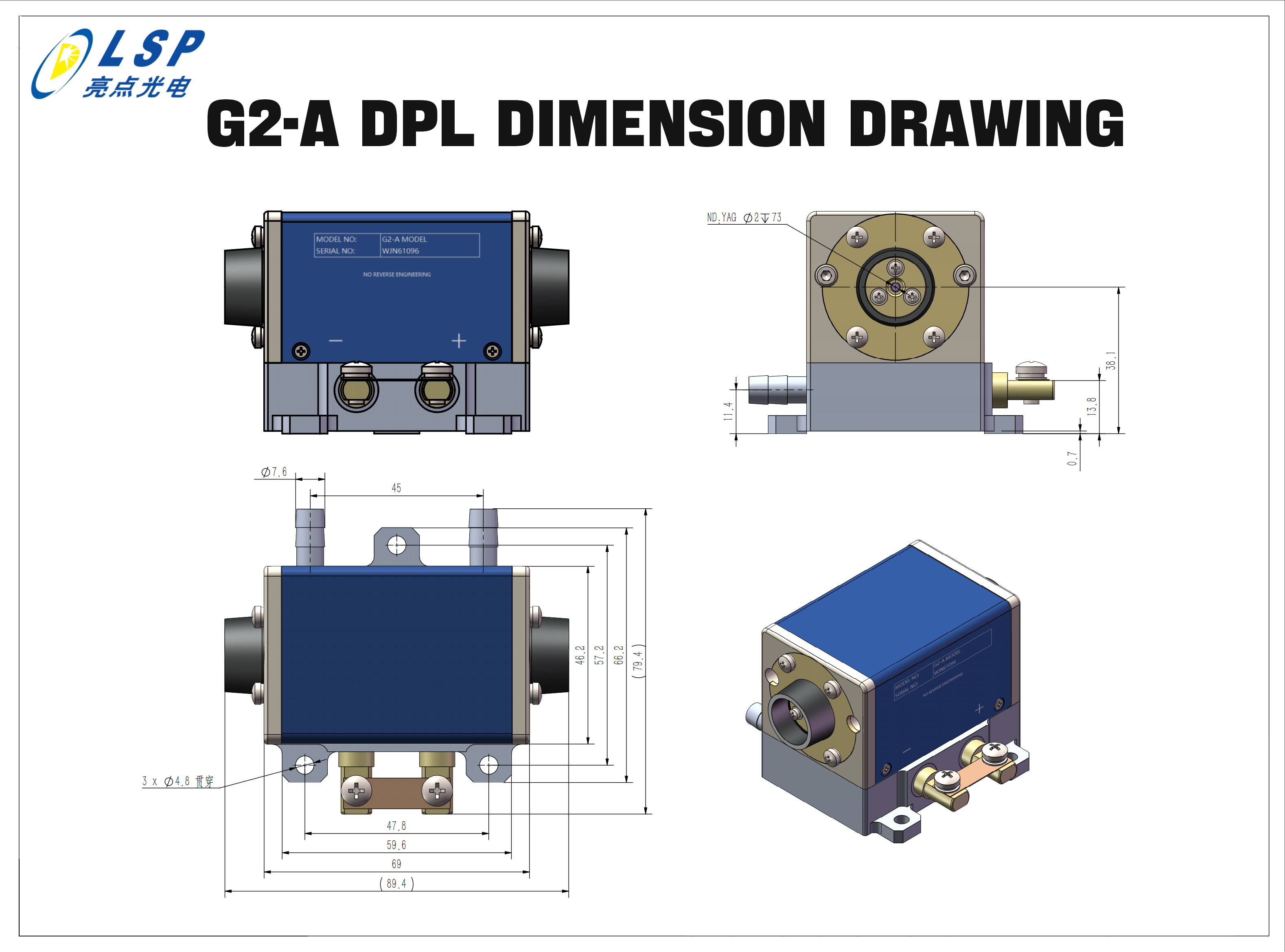
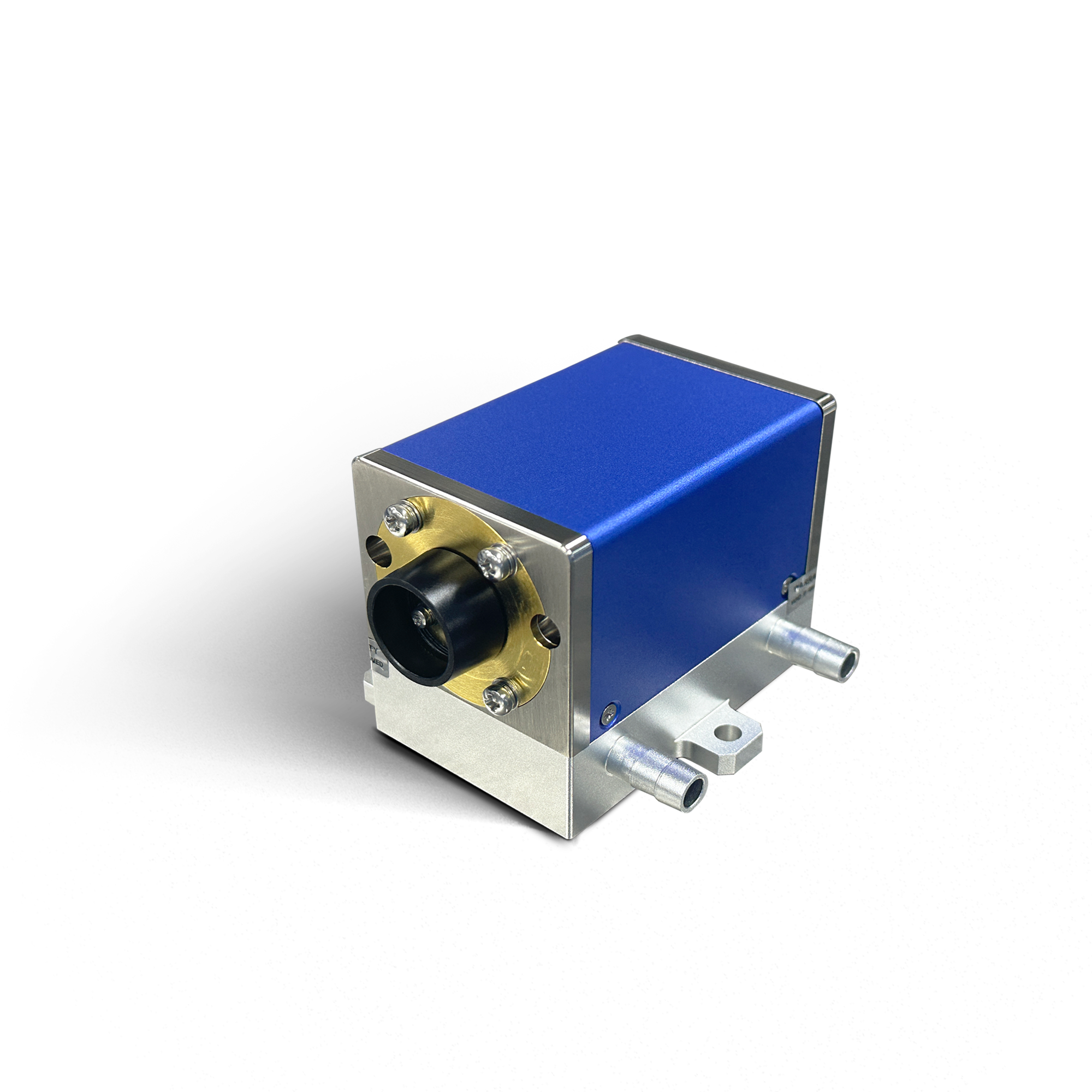
Product Bundle Set of G2-A DPL From Lumispot Tech
Each set of products contains three groups of horizontally stacked array modules, each group of Horizontal Stacked Array modules pumping power of about 100W@25A, and an overall pumping power of 300W@25A.
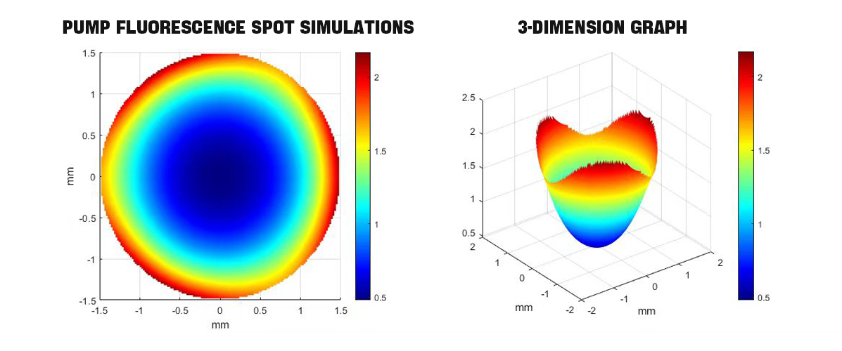
The G2-A pump fluorescence spot is shown below:
The Main Technical Data Of G2-A Diode Pump Solid State Laser :
Our Strength In Technologies
1. Transient Thermal Management Technology
Semiconductor-pumped solid-state lasers are widely used for quasi-continuous wave (CW) applications with high peak power output and continuous wave (CW) applications with high average power output. In these lasers, the height of the thermal sink and the distance between chips (i.e., the thickness of the substrate and the chip) significantly influence the heat dissipation capability of the product. A larger chip-to-chip distance results in better heat dissipation but increases the product volume. Conversely, if the chip spacing is reduced, the product size will be reduced, but the product's heat dissipation capability may be insufficient. Utilizing the most compact volume to design an optimal semiconductor-pumped solid-state laser that meets the heat dissipation requirements is a difficult task in the design.
Graph Of The Steady-state Thermal Simulation
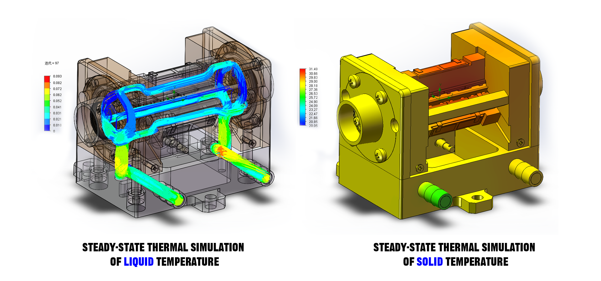
Lumispot Tech applies the finite element method to simulate and calculate the temperature field of the device. A combination of solid heat transfer steady-state thermal simulation and liquid temperature thermal simulation is used for thermal simulation. For continuous operation conditions, as shown in the figure below: the product is proposed to have the optimal chip spacing and arrangement under the solid heat transfer steady-state thermal simulation conditions. Under this spacing and structure, the product has good heat dissipation capability, low peak temperature, and the most compact characteristic.
2. AuSn solder encapsulation process
Lumispot Tech employs a packaging technique that utilizes AnSn solder instead of traditional indium solder to address issues related to thermal fatigue, electromigration, and electrical-thermal migration caused by indium solder. By adopting AuSn solder, our company aims to enhance product reliability and longevity. This substitution is carried out while ensuring constant bar stacks spacing, further contributing to the improvement in product reliability and lifespan.
In the packaging technology of high-power semiconductor pumped solid-state laser, indium (In) metal has been adopted as the welding material by more international manufacturers due to its advantages of low melting point, low welding stress, easy operation, and good plastic deformation and infiltration. However, for semiconductor pumped solid state lasers under continuous operation application conditions, the alternating stress will cause stress fatigue of the indium welding layer, which will lead to product failure. Especially in high and low temperatures and long pulse widths, the failure rate of indium welding is very obvious.
Comparison of accelerated life tests of lasers with different solder packages
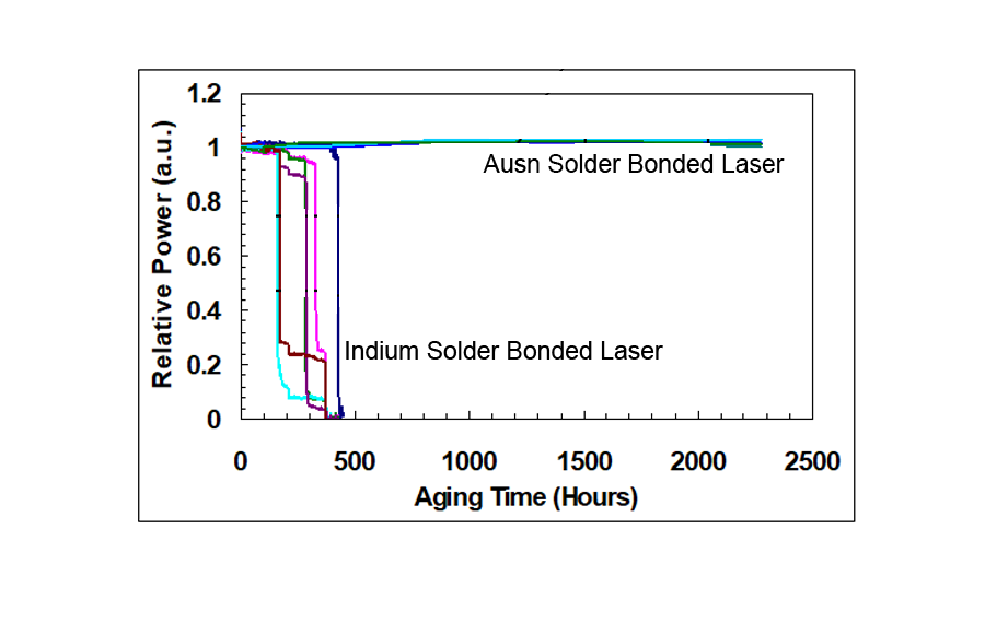
After 600 hours of aging, all the products encapsulated with indium solder fail; while the products encapsulated with gold tin work for more than 2,000 hours with almost no change in power; reflecting the advantages of AuSn encapsulation.
In order to improve the reliability of high-power semiconductor lasers while maintaining the consistency of various performance indicators, Lumispot Tech adopts Hard Solder (AuSn) as a new type of packaging material. The use of coefficient of thermal expansion matched substrate material (CTE-Matched Submount), the effective release of thermal stress, a good solution to the technical problems that may be encountered in the preparation of hard solder. A necessary condition for the substrate material (submount) to be able to be soldered to the semiconductor chip is surface metallization. Surface metallization is the formation of a layer of diffusion barrier and solder infiltration layer on the surface of the substrate material.
Schematic diagram of the electromigration mechanism of a laser encapsulated in indium solder
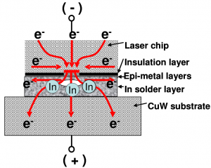
In order to improve the reliability of high-power semiconductor lasers while maintaining the consistency of various performance indicators, Lumispot Tech adopts Hard Solder (AuSn) as a new type of packaging material. The use of coefficient of thermal expansion matched substrate material (CTE-Matched Submount), the effective release of thermal stress, a good solution to the technical problems that may be encountered in the preparation of hard solder. A necessary condition for the substrate material (submount) to be able to be soldered to the semiconductor chip is surface metallization. Surface metallization is the formation of a layer of diffusion barrier and solder infiltration layer on the surface of the substrate material.
Its purpose is on the one hand to block the solder to the substrate material diffusion, on the other hand is to strengthen the solder with the substrate material welding ability, to prevent the solder layer of the cavity. Surface metallization can also prevent the substrate material surface oxidation and moisture intrusion, reduce the contact resistance in the welding process, and thus improve the welding strength and product reliability. The use of hard solder AuSn as the welding material for semiconductor pumped solid state lasers can effectively avoid indium stress fatigue, oxidation and electro-thermal migration and other defects, significantly improving the reliability of semiconductor lasers as well as the service life of the laser. The use of gold-tin encapsulation technology can overcome the problems of electromigration and electrothermal migration of indium solder.
Solution From Lumispot Tech
In continuous or pulsed lasers, the heat generated by the absorption of pump radiation by the laser medium and the external cooling of the medium lead to uneven temperature distribution inside the laser medium, resulting in temperature gradients, causing changes in the refractive index of the medium and then producing various thermal effects. The thermal deposition inside the gain medium leads to the thermal lensing effect and thermally induced birefringence effect, which produces certain losses in the laser system, affecting the stability of the laser in the cavity and the quality of the output beam. In a continuously running laser system, the thermal stress in the gain medium changes as the pump power increases. The various thermal effects in the system seriously affect the whole laser system to obtain better beam quality and higher output power, which is one of the problems to be solved. How to effectively inhibit and mitigate the thermal effect of crystals in the working process, scientists have been troubled for a long time, it has become one of the current research hotspots.
Nd:YAG laser with thermal lens cavity

In the project of developing high-power LD-pumped Nd:YAG lasers, the Nd:YAG lasers with thermal lensing cavity were solved, so that the module can obtain high power while obtaining high beam quality.
In a project to develop a high-power LD-pumped Nd:YAG laser, Lumispot Tech has developed the G2-A module, which greatly solves the problem of lower power due to thermal lens-containing cavities, allowing the module to obtain high power with high beam quality.
Post time: Jul-24-2023


