With the rapid development of optoelectronic technology, semiconductor lasers have found widespread applications in fields such as communications, medical equipment, laser ranging, industrial processing, and consumer electronics. At the core of this technology lies the PN junction, which plays a vital role—not only as the source of light emission but also as the foundation of the device’s operation. This article provides a clear and concise overview of the structure, principles, and key functions of the PN junction in semiconductor lasers.
1. What is a PN Junction?
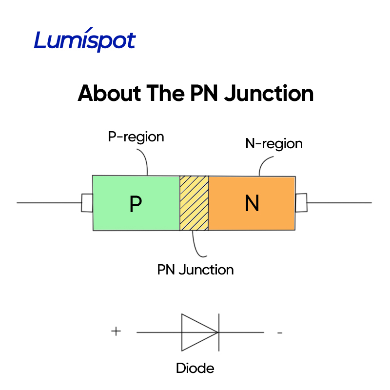
A PN junction is the interface formed between a P-type semiconductor and an N-type semiconductor:
P-type semiconductor is doped with acceptor impurities, such as boron (B), making holes the majority charge carriers.
The N-type semiconductor is doped with donor impurities, such as phosphorus (P), making electrons the majority carriers.
When the P-type and N-type materials are brought into contact, electrons from the N-region diffuse into the P-region, and holes from the P-region diffuse into the N-region. This diffusion creates a depletion region where electrons and holes recombine, leaving behind charged ions that create an internal electric field, known as a built-in potential barrier.
2. The Role of the PN Junction in Lasers
(1) Carrier Injection
When the laser operates, the PN junction is forward biased: the P-region is connected to a positive voltage, and the N-region to a negative voltage. This cancels the internal electric field, allowing electrons and holes to be injected into the active region at the junction, where they are likely to recombine.
(2) Light Emission: The Origin of Stimulated Emission
In the active region, injected electrons and holes recombine and release photons. Initially, this process is spontaneous emission, but as the photon density increases, photons can stimulate further electron-hole recombination, releasing additional photons with the same phase, direction, and energy—this is stimulated emission.
This process forms the foundation of a laser (Light Amplification by Stimulated Emission of Radiation).
(3) Gain and Resonant Cavities Form Laser Output
To amplify stimulated emission, semiconductor lasers include resonant cavities on both sides of the PN junction. In edge-emitting lasers, for example, this can be achieved using Distributed Bragg Reflectors (DBRs) or mirror coatings to reflect light back and forth. This setup allows specific wavelengths of light to be amplified, eventually resulting in highly coherent and directional laser output.
3. PN Junction Structures and Design Optimization
Depending on the type of semiconductor laser, the PN structure may vary:
Single Heterojunction (SH):
The P-region, N-region, and active region are made of the same material. The recombination region is broad and less efficient.
Double Heterojunction (DH):
A narrower bandgap active layer is sandwiched between the P- and N-regions. This confines both carriers and photons, significantly improving efficiency.
Quantum Well Structure:
Uses an ultra-thin active layer to create quantum confinement effects, improving threshold characteristics and modulation speed.
These structures are all designed to enhance the efficiency of carrier injection, recombination, and light emission in the PN junction region.
4. Conclusion
The PN junction is truly the “heart” of a semiconductor laser. Its ability to inject carriers under forward bias is the fundamental trigger for laser generation. From structural design and material selection to photon control, the performance of the entire laser device revolves around optimizing the PN junction.
As optoelectronic technologies continue to advance, a deeper understanding of PN junction physics not only enhances laser performance but also lays a solid foundation for the development of the next generation of high-power, high-speed, and low-cost semiconductor lasers.
Post time: May-28-2025